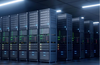
In the digital economy era, AI and big data technologies are reshaping the global industrial landscape. According to a McKinsey report, the global AI market will reach $1.5 trillion in 2024, with a compound annual growth rate (CAGR) exceeding 25%. International Data Corporation (IDC) predicts that global spending on big data analytics will exceed $300 billion over the next two years, driving exponential growth in demand for data center servers.

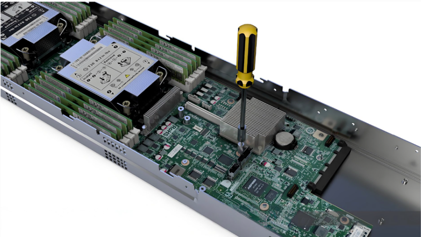
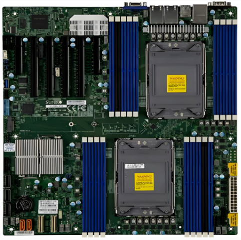
At the heart of all this is server motherboards—they serve as the "brains" of AI systems. Consequently, the printed circuit boards (PCBs) used for AI computing have become the lifeblood of the electronics industry. These motherboards must host high-speed chips like CPUs and GPUs, ensuring real-time processing of massive amounts of data. However, the design and manufacturing requirements for these PCBs are extremely high: they require a 18-layer, 4-8-level HDI (high-density interconnect) structure and high-frequency, high-speed materials as the substrate. Unfortunately, manufacturers capable of producing these high-end PCBs are currently scarce, especially in the areas of prototype and small-batch manufacturing, severely hindering the pace of innovation in the AI era.
As a leading company with a decade of experience in HDI PCB manufacturing, MASSIVE PCB has focused on high-reliability and high-precision manufacturing.We have continuously enhanced our technology in the field of small- medium-volume manufacturing, gradually filling gaps in several challenging HDI PCB manufacturing processes. Leveraging a decade of expertise in fine-wire and microvia technologies.
This article will start with the current state of the AI trend, deeply analyze the characteristics of server substrate PCBs, supply bottlenecks, and solutions provided by MASSIVE PCB, and look forward to the future development blueprint. It calls on the industry to work together to promote the transformation of the AI electronics industry and contribute its valuable strength to the domestic substitution of large server substrates.

Industry status and demand data
Artificial intelligence and big data technologies are now entering large-scale commercial use. IDC data shows that the global AI server market will reach US$30.7 billion in 2023, a year-on-year growth of 35.6%. It is projected to exceed US$90 billion by 2028, with a compound annual growth rate of 24%. Cluster servers used for training large models place particularly stringent hardware requirements, requiring each GPU node to be equipped with an ultra-high-performance motherboard. For example, NVIDIA's DGX SuperPOD system uses an 8-level HDI PCB motherboard to support petabyte-level data throughput.
Big data analytics is also driving demand. According to Statista, the global data platform, the total amount of data will reach 120 zettabytes (1 zettabyte = 1 billion terabytes) in 2023 and will increase to 180 zettabytes by 2025. Cloud computing giants like Amazon AWS and Microsoft Azure will need to deploy millions of servers: Google's data centers alone will add over 1 million servers in 2023, a 28% increase over the previous year. These server motherboards must support high-frequency computing (such as 128-core CPUs running at frequencies above 5GHz) and low-latency transmission, making PCBs with 18 or more layers the standard. A report by industry research firm Prismark indicates that the high-end server PCB market will reach $18 billion in 2023, with 18-24 layer PCBs accounting for over 60%. Demand is expected to increase to $25 billion by 2025, with an annual growth rate exceeding 20%.
Specific demand data are as follows,
★Layer Count Requirements: The average number of layers in AI server motherboards will jump from 14 in 2019 to 18-22 in 2024. Dell PowerEdge series motherboards have adopted a 20-layer design to meet AI inference loads.
★High-frequency and high-speed: As signal frequencies rise above 112Gbps (e.g., PCIe 5.0), substrate materials must have a dielectric constant (Dk) <3.5 and a dissipation factor (Df) ≤ 0.002.
★Market gap: The global demand gap will be as high as 18% in 2024, and the delivery delay rate of small-batch orders (less than 500 pieces) will be as high as 060%, which will greatly delay the launch cycle of server products.
This trend stems from the AI industry's "Law of Accelerated Innovation": the cycle time from prototype to mass production has been shortened to 3-6 months. However, the PCB substrates that underpin all of this have become a bottleneck in the industry's development. Only high-density, high-frequency, high-speed, high-order, and highly reliable HDI PCBs can meet product demands, but their manufacturing process is a Mount Everest in the small- and medium-volume PCB manufacturing industry. Next, we will analyze their core characteristics in detail.

Unveiling the Characteristics and Manufacturing of Server PCB Substrates
PCB substrates for large AI servers are the pinnacle of electronics manufacturing. Their characteristics can be summarized as "five highs": high-rise (>18 layers), high-frequency signals (GHz-level transmission), high-speed data (Gb/s-level speeds), high-order (4-8th-order HDI structure), and high density (line width/spacing <50μm). Take a typical 8-level HDI server motherboard as an example: 20 layers of copper foil are stacked, interconnected by millions of microvias, supporting 128 high-density BGA chips, with an overall thickness of less than 2mm. High-frequency and high-speed substrates such as Rogers RO-300B, TU-5785N, and Taiyao TU883, which dominate the market, must maintain a stable Dk value within 3.4±0.05.
The core product features are as follows:
★High-layer structures (18-30 layers): Multi-layer stacking ensures power integrity. For example, a 24-layer PCB requires 12 signal layers, 8 power layers, and 4 ground layers to reduce noise interference. The key technical point is inter-layer alignment accuracy (error <5μm). A deviation exceeding 10μm will increase signal reflectivity by 15%, causing AI calculation errors.
★High-frequency and high-speed characteristics: The frequency is increased to 5-10 GHz to support DDR5 memory (6.4 Gbps bandwidth). The difficulty lies in dielectric control. The material must have a Df < 0.002 at 10 GHz, otherwise signal loss will increase dramatically (for example, if the loss is > 3 dB/inch, the transmission distance is halved). High-speed transmission relies on impedance consistency (100 Ω + 5%), requiring precise calculation of differential pair line width (+ 2 μm error) to avoid increased bit error rates in data centers.
★High-order HDI (4-8): High-order means ultra-microvia interconnect structures. 4-order HDI requires four laser drilling passes, with apertures ≤ 0.1mm; 8-order HDI requires eight stacked laser drilling passes. At high density, the number of microvias per square inch exceeds 5,000.
★High-density interconnects: Line width/spacing is reduced to less than 50μm/50μm (the diameter of a human hair is approximately 70μm), with pin density reaching 200 pins/cm. This requires "zero blind via" technology—integrated blind and buried through-holes on all layers—to ensure low signal latency (<10ps/inch).
Manufacturing process difficulties and technical key points:
The process of producing this type of PCB is comparable to the art of micro-carving. Its key technical points are mainly reflected in the following four aspects:
★Interlayer alignment and stacking control: PCBs with more than 18 layers require 3+ presses, which can easily cause layer deviation and short circuits.
★Microvia technology: Laser drilling requires drilling through 2-4 mil apertures, which can easily lead to "taper defects" and "hole-pad separation," affecting conductivity. The key technology is pulse energy control: when the energy is <20pJ/pulse, the success rate exceeds 98%.
★Signal integrity assurance: The skin effect is enhanced at high frequencies, requiring "gold plating" (electroless gold plating + nickel-gold plating) to ensure zero impedance stability. The challenge lies in plating uniformity (±0.05μm variation).
★Material thermal management: The coefficient of thermal expansion (CTE) of high-frequency materials must match that of copper foil (16ppm/°C). Otherwise, the risk of delamination during high-temperature reflow soldering increases by 40%.
Behind these technological difficulties lies a deep investment black hole: a single high-end HDI PCB production line requires an investment of over 50 million RMB. Without years of technological development, achieving reliable mass production is nearly impossible. MASSIVE PCB utilizes a "four-step process" (precision drilling, high-layer lamination, high-precision etching, and signal testing) to increase yield to over 95%.
Supply Status of PCB Substrates for Servers
AI innovation is exposing supply chain shortcomings. Prismark's 2023 report shows that fewer than 10 PCB factories worldwide can consistently mass-produce high-end HDI motherboards with 18 or more layers, with 90% of production capacity monopolized by overseas giants like Samsung and TTM. The remaining manufacturers focus on large-volume orders (over 10,000 pieces), leaving prototypes and small-batch manufacturing (1-500 pieces) in a vacuum. The supply-demand gap is as high as 30%, and 80% of AI startups report motherboard delivery delays of 7-9 weeks.
Supply shortage data is shown below,
★Unbalanced capacity distribution: In 2024, the average delivery cycle of samples and small batch boards in the global high-end HDIPCB production capacity will be extended to 8 weeks (the standard is 2-4 weeks).
★Cost and economic barriers: Small-batch trial production requires resetting the production line, which increases costs by 60%. Small and medium-sized factories are deterred by the extremely high equipment investment.
★Technical threshold restrictions: 40% of PCB factories are blocked from manufacturing server substrates due to insufficient stacking control and microvia technology.
★Regional concentration: 70% of production capacity is concentrated in Taiwan and South Korea (such as Samsung and Unimicron). The absence of European and American suppliers creates tariff risks. Geopolitical conflicts in 2023-2024 could cause import cycles and costs for sample and small-batch server substrates to surge by over 30%.
The root cause of the shortage lies in the "three highs paradox": high investment (¥50 million per line), high risk (20% sample failure rate), and high technical barriers (the "five highs" characteristic). Sample shortages directly stifle innovation. Tesla's AI director has publicly criticized PCB suppliers for hindering the development of Autopilot. Against this backdrop, MASSIVE PCB, through dedicated research, has pioneered the domestic production of small and medium-volume server substrates.
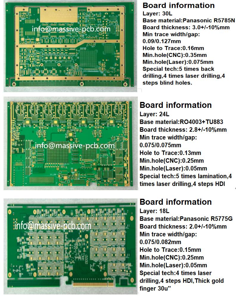
As a pioneer in China's high-difficulty HDI PCB (High-Definition Circuit) market, MASSIVE PCB has been committed to its mission of "high reliability and high precision". The company's product research institute's technical team focuses on the server motherboard segment, and over a decade of development has forged four key technological pillars: fine-wire technology, interlayer alignment technology, microvia technology, and signal integrity control technology.
The following are some products of server substrates produced by us.

The future is here. Every 1% growth in the AI server market will require tens of millions of high-performance PCBs. MASSIVE PCB is committed to using technology as our driving force to continue filling gaps and accelerating the implementation of innovation. We sincerely invite partners worldwide—whether you're an AI maker or a cloud giant—to join us on this journey. Let every engineering prototype and small-batch server motherboard become the spark that drives the intelligent world.
Let us work together to help the AI electronics industry enter a golden decade of limitless possibilities.
Post on 6-August-2025


